The kSA MOS UltraScan and kSA MOS ThermalScan systems are ex situ, flexible, high-resolution scanning curvature, bow, and tilt-measurement systems.
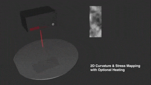 The kSA MOS UltraScan and kSA MOS ThermalScan systems are flexible, high-resolution scanning curvature, bow, and tilt-measurement systems. Based on proven and patented kSA MOS technology, the kSA MOS UltraScan uses a laser array to map the two-dimensional curvature, wafer bow, and stress of semiconductor wafers, optical mirrors, glass, lenses – practically any polished surface. For room temperature measurements, explore the kSA MOS UltraScan. If you want to know how your wafer changes with temperature, explore the kSA MOS ThermalScan.
Videos
Have a measurement challenge in mind?
One of the pillars of our success is standing by as consultants. We’re always here to talk about your project needs.
© 2026 IBT Online