Metalorganic Chemical Vapor Deposition (MOCVD)
Increase performance and quality with compact in situ tools for MOCVD. Discover the power of feedback control of wafer carrier/pocket temperature, film thickness, thin-film stress/wafer bow, and surface measurement in real-time.
 Metalorganic Chemical Vapor Deposition (MOCVD), sometimes called Metalorganic Vapor Phase Epitaxy (MOVPE), is a much higher throughput technique compared with MBE, and as such is the production deposition tool of choice for most compound semiconductor devices such as High Brightness LED’s (HBLED). Worldwide, there are several research-level MOCVD tool manufacturers, including Structured Materials, Taiyo Nippon-Sanso, Valence Process Equipment, Samco and others. However, at the production level, there are two companies that dominate sales and have over 90 percent of the collective market share: Veeco Turbodisc and Aixtron.
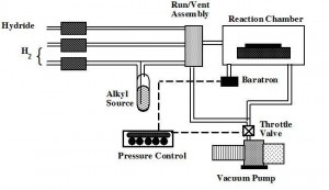
MOCVD relies on the gas phase transfer of the materials to be deposited on the substrate. The deposition ultimately occurs via a chemical reaction at the substrate surface and typically results in high quality, epitaxial thin-film deposition. Because MOCVD utilizes heated gas flow and surface chemical reaction, substrate temperatures for typical device growth are higher than MBE and in the 500-1500 degrees Celcius range. In addition, the sample can be rotated at speeds as high as 1500 RPM to promote higher uniformity and film quality. Furthermore, optical access is typically limited to less than 10mm, and the optical path distance is typically short (e.g. 250mm or less). In addition, MOCVD deposition occurs at pressures close to atmospheric pressure, which precludes in situ metrology that utilize electron beams or x-rays. For these reasons, in situ optical metrology probes for MOCVD are typically compact in size. The kSA ICE metrology tool is small, compact, and easy to use. This tool offers in situ direct substrate temperature, wafer carrier temperature, film thickness, thin-film stress/wafer curvature, and surface roughness measurement in real-time.
Related Metalorganic Chemical Vapor Deposition (MOCVD) Products


Have a measurement challenge in mind?
One of the pillars of our success is standing by as consultants. We’re always here to talk about your project needs.
© 2026 IBT Online